Scanning Tunneling Microscopy (STM)
The scanning tunneling microscope (STM) is an important method for studying surfaces of conducting materials on an atomic scale. The method is based on the quantum mechanical tunneling effect, which allows electrons to penetrate potential barriers even though their energy is classically insufficient to do so. In scanning tunneling microscopy, this effect is exploited between a tip and a conductive sample. The potential barrier here is the vacuum between the tip and the sample.
By bringing the tip closer to the sample and applying a voltage, a tunnel current can be generated. The tunnel current is kept constant in an electronic control loop by readjusting the distance between the tip and the sample. Imaging is then performed by the deflection of the tip, which follows the surface structure. Thereby, at the position of an atom, a high deflection is imaged as a bright color and at a defect, a low deflection is imaged as a dark color. By scanning the sample surface with the tunnel tip, the position of atoms on the surface is thus displayed.

Scanning tunneling microscopy offers a high vertical resolution of a few picometers and a lateral resolution in the subnanometer range. Quantum mechanics justifies this high resolution by the strong dependence of the tunnel current on the distance between tip and sample. For example, a change of the distance by only 1 Å leads to a change of the tunnel current by one order of magnitude.
RT-STM

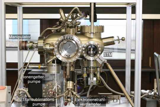
This setup consists of a room temperature scanning tunneling microscope (RT-STM) in an ultra high vacuum (UHV) chamber. There is no possibility to cool or heat the samples during the measurement.
Metal substrates as well as semiconductor samples can be prepared and examined in the STM. The samples are held by a manipulator equipped with a heatable holder for preparation to obtain temperatures of max. 1500 °C. The manipulator can heat metal substrates resistively via a filament and semiconductors via direct current. Furthermore, metals or molecules can be evaporated by means of an electron beam evaporator or a Knudsen cell. Furthermore, the apparatus also has a LEED, which makes it possible to investigate periodicities and symmetries of the adsorbate structure in momentum space.
VT-STM

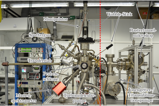
Another UHV setup is equipped with a variable temperature scanning tunneling microscope (VT-STM). The VT-STM offers the possibility to examine samples in a temperature interval of 10-1400K. The measuring tip is kept at room temperature and the sample is cooled or heated, thus temperature dependent effects can be investigated.
This apparatus is divided into two units separated by a slide valve. It consists of the measuring section on the right side with the VT-STM and the preparation chamber on the left side. In the preparation chamber, a manipulator with resistive sample heating and direct current heating is available. There, samples can be cooled down to 100K and analyzed with a LEED system. The chemical composition of the samples can be investigated via Auger electron spectroscopy.


