Low-Energy Electron Diffraction (LEED)
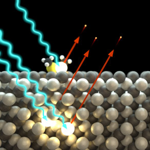
Electrons can be diffracted like photons due to their wave properties. In the context of low-energy electron diffraction, kinetic energies around 100eV and thus wavelengths of 1.2Å are typically used. The penetration depth of free electrons is very small. For inelastic collisions with sample atoms, it is largely independent of the material and changes only with the kinetic energy of the electrons. Due to the low penetration depth, only surface information of the uppermost layers is determined.
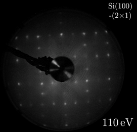
The electrons used here originate from a directly or indirectly heated cathode, are focused via electron lenses and finally accelerated to the final energy set on the instrument. The sample is struck perpendicularly so that the electrons are backscattered in the same direction. They pass through at least two gratings. Only elastically scattered electrons are of interest for the evaluation, inelastic electrons can be filtered beforehand by decelerating fields. The electrons which have passed the last grating are accelerated towards a luminescent screen which represents the diffraction pattern. For the measurement it is sufficient to pass only the electron energy to obtain all possible diffraction patterns of the crystal instantaneously. Passing through azimuth angles is not necessary.

Low-energy electron diffraction therefore contributes a fast and simple way to characterize the periodic arrangement of the sample. In addition, information about surface defects and the local structure of the sample can be obtained from the intensity profile of the observed reflections and the energy-dependent modulation of the intensities (IV-LEED).


